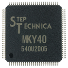
MKY40 (Discontinued products)

|
■Discontinued November 30, 2021 |
|
|
CUnet master IC, 5 V The MKY40 is a CUnet IC that has two functions, one for MEM mode (master/slave) and one for IO mode (slave). However, it has been more than 10 years since the MKY40 was released. We now have the MKY43 for MEM mode and the MKY46 for IO mode. We recommend that you use these new ICs instead of the MKY40 for new designs. |
||
If the MKY40 in MEM mode is connected to a CPU using an 8-bit, 16-bit, or 32-bit bus, it can be accessed from the CPU. Also, the MKY40 can be used as either a master or a slave terminal on a CUnet network. The MKY40 contains 512 bytes of shared memory, a buffer for its mail function, and a communication control register.
[512 bytes of shared memory]
The 512-byte shared memory consists of 64 blocks (8 bytes per block). This 512-byte shared memory consists of a "self-owned area" to which only the CPU connected to the CUnet IC can write, and an area where input data from other CUnet ICs is copied.
The MKY40 can specify the number of blocks to use (the self-owned area). The data written by the CUnet IC and the input data from other CUnet ICs are both reflected in the 512 bytes of shared memory of the CUnet IC. This makes it easy to grasp the entire CUnet network just by reading the shared memory of the CUnet IC connected to the CPU.
[Mail function buffer]
The mail function buffer consists of two receiving buffers and one sending buffer. Each buffer is 256 bytes.
[Communication control register]
This register controls communication, including communication start, error checking, mail sending and receiving, etc. CUnet communication can be controlled easily just by accessing this register. Also, the MKY40 has two interrupt pins. They enable a variety of interrupt functions such as shared memory update interrupts, mail send interrupts, mail receive complete interrupts, specific terminal connection interrupts, specific terminal disconnection interrupts, and communication error interrupts.
In addition to this wealth of interrupt functions, the MKY40 also contains built-in communication protocol, allowing it to relieve the load on the CPU for communication functions.
[Difference between the MKY40 in IO mode and the MKY46]
The MKY46 can replace an MKY40 that is used in IO mode.
[Difference between the MKY40 in MEM mode and the MKY43]
Our lineup includes the MKY43, MEM mode, 3.3 V, which can replace the functions of the MKY40 in MEM mode. The MKY43 works and functions just like the MKY40, but please observe the following practical differences in its use.
Differences between MKY40 (MEM mode) and MKY43
| Model | MKY43 | MKY40 |
|---|---|---|
| Power supply voltage | 3.3 V | 5.0 V |
| Package | 0.5-mm pitch 64 pins TQFP | 0.5-mm pitch 100 pins TQFP |
| Bus pin level | 3.3 V TTL (5 V tolerant) (5.0 V TTL level CPU bus can be connected.) |
5.0 V TTL level |
| Bus width | 16 bits / 8 bits | 32 bits / 16 bits / 8 bits |
| Byte write when 16-bit user bus is connected | Byte write is not supported (For write access, set both #WRH pin and #WRL pin Low level.) |
Byte write is supported. |
| Interrupt pin | #INT0, #INT1 | #INT0, #INT1, #INT2 |
| Port Out bit of SSR Care Pulse bit of BCR |
Not provided | PO0, PO1, PO2, PO3 (SSR) CP (BCR) |
| Setting pin for address, etc. (Initial value of BCR is written) |
Not provided | #SA0 to #SA5, #OWN0 to #OWN5, BPS0, BPS1 |
| IO mode function | Not provided | Provided (The MODE pin is provided.) |
| CYCT output, PING output (CYCT is equivalent to STB) |
#CYCT signal and #PING signal can be output to UTY1 pin and UTY2 pin. | #STB signal and PING signal are output to #STB pin and PING pin respectively |
| UTCR (UTility pin Control Register) |
Added for controlling UTY1 pin and UTY2 pin. (Set this register by selecting from among Hi-Z, #CYCT output, and #PING output.) |
------- |
| Driving clock | Clock input to the Xi pin (The oscillator is not supported.) |
Clock input to the Xi pin. Or the crystal oscillator between the Xi pin and Xo pin can be supported. |
| TXD pin output during reset period |
Low level | Clock frequency obtained by dividing the driving clock by 32 |
| Hazard protection | Hazard-protection-buffer method | Window-lock method |
| Memory map and endian | Different from that of the MKY40 | ------- |
| Address of each register | Different from that of the MKY40 | ------- |
| Bus access time | TRD (max) 89 ns | TRD (max) 130 ns |
| Operating current (max) | 75 mA | 130 mA |
MKY40 (MEM mode)
| Bus width | 8 bits / 16 bits / 32 bits |
|---|---|
| Control terminal | CS, RD, WRLL, WRLH, WRHL, WRHH |
| Interrupt pin | 3 pins |
| CPU voltage | 5.0 V |
MKY40 (IO mode)
| DIO | 32 bits (Settable I/O by 4 bits) |
|---|
| Communication method | CUnet communication |
|---|---|
| Communication rate | 3/6/12 Mbps (half duplex) |
| Package | TQFP 100-pin |
| Package dimensions | 16×16×1.7 mm (0.5 mm pitch) |
| Operating ambient temperature |
-40 to +85℃ |
| Supply voltage | 5.0 V |
| External input operating frequency |
48 MHz |
